Nikon XT V Series
- Model
- XT V Series
- Category
- X-ray CT
- Solutions
- Industrial Metrology and Quality Inspection
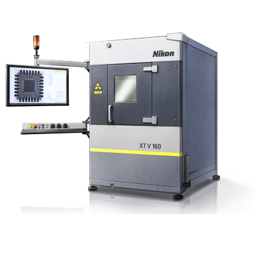
The XT V series enables insights into printed circuit board assemblies, components, or electrical devices in an intuitive, non-destructive inspection process. X-ray inspection provides many benefits to manufacturers and researchers alike, accelerating throughput and improving product quality – all whilst reducing costs. Set up an automated inspection program in minutes with the intuitive Inspect-X interface – no programming required! PCB Analysis Suite is capable of advanced measurement and analysis of BGA, bond wires, PTH and complex packages such as PoP on multi-layered boards, with automated pass/fail inspection and reporting.
Overview
The XT V series enables insights into printed circuit board assemblies, components, or electrical devices in an intuitive, non-destructive inspection process. X-ray inspection provides many benefits to manufacturers and researchers alike, accelerating throughput and improving product quality – all whilst reducing costs. Set up an automated inspection program in minutes with the intuitive Inspect-X interface – no programming required! PCB Analysis Suite is capable of advanced measurement and analysis of BGA, bond wires, PTH and complex packages such as PoP on multi-layered boards, with automated pass/fail inspection and reporting.
Applications: Large-volume dimensional inspection · Machine tool and robot calibration · Reverse engineering · Internal defect inspection with CT · Small-part optical measurement
Technical specifications
| Maximum kV | 160 kV / 130 kV |
|---|---|
| X-ray source | Open tube with replaceable filaments for unlimited lifetime |
| High voltage generator | Integrated generator - no HV cable maintenance required |
| Feature recognition | Submicron / Micron-level |
| Viewing angle range | Up to 82° in any direction / Up to 79° in any direction |
| Sample tray | Carbon fibre tray, 580 mm (22.8 ") diameter |
| Cabinet dimensions (W x D x H) | 1,260 x 1,789 x 1,904 mm (50 x 70 x 75 ") |
| System weight | 2,100 kg (4,630 lbs) |
| ESD safety | ESD-safe to industry standards with optional ESD Safety Upgrade |
| Primary applications | Automated and real-time electronics and semiconductor inspection for R&D, QA, QC and failure analysis / Real-time electronics inspection |

Solutions
Industrial Metrology and Quality Inspection
Laser trackers, measuring arms, laser radar, X-ray CT and optical measuring for manufacturing quality.
Related products
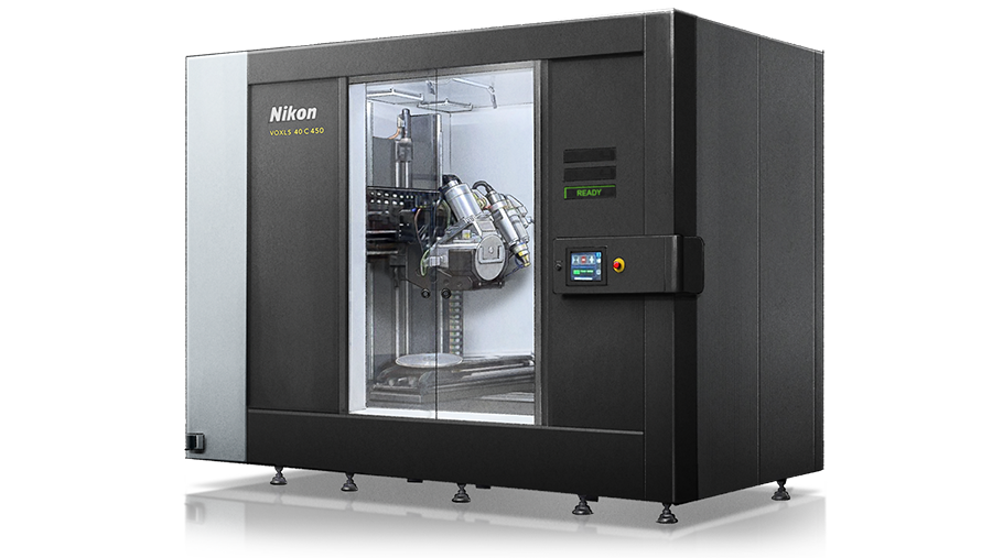
Nikon Large Envelope X-ray CT
Nikon’s advanced, large envelope X-ray and CT systems provide ultimate versatility for inspecting small and large parts. Nikon’s versatile, large-envelope X-ray and CT systems can
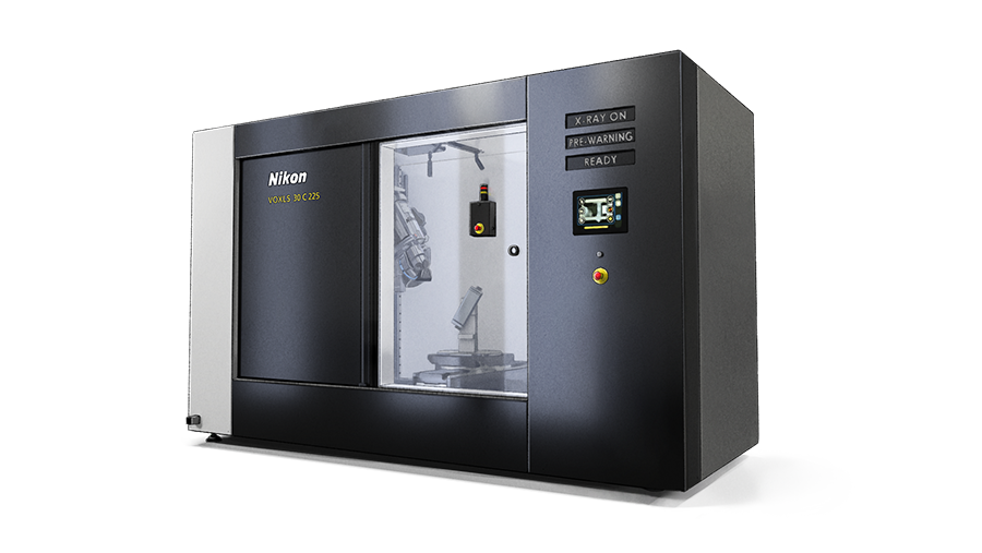
Nikon VOXLS 30 Series
Nikon’s advanced, large envelope X-ray and CT systems provide ultimate versatility for inspecting small and large parts. Nikon’s VOXLS 30 Series systems deliver automation readine
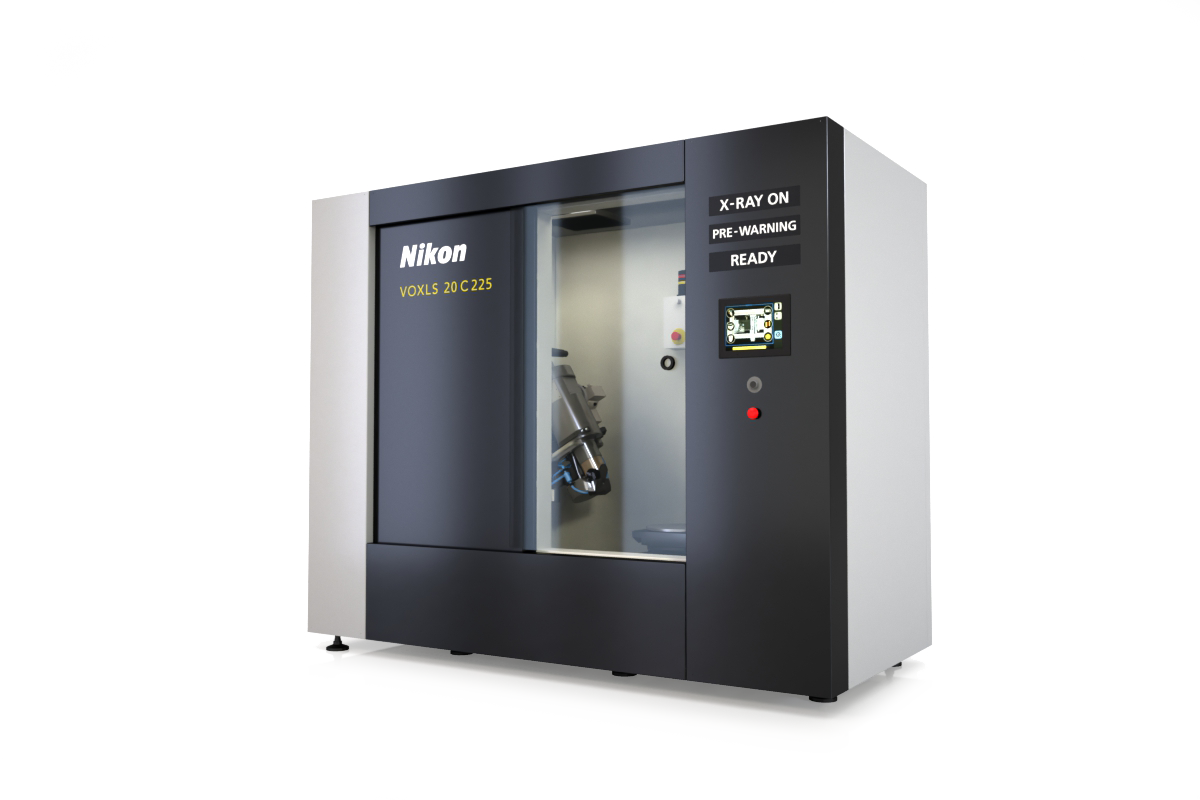
Nikon VOXLS 20 Series
Nikon’s VOXLS 20 Series systems deliver industry-leading CT inspection capability in a space-efficient footprint, paired with scan energies up to 225 kV, making it an ideal solutio
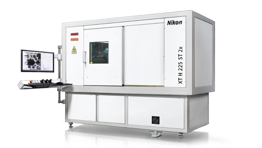
Nikon XT H Series
Nikon's versatile microfocus CT systems for high-resolution inspection of components in R&D, failure analysis and production quality control. These systems combine the adaptabilit